
| 
| 
|
|
|
|
|
In-Page links
| |||
| NTP | LED Matrix | RTC | ESP01 |
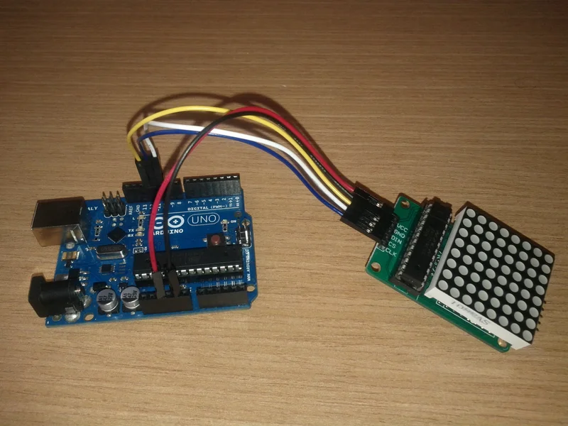
The MAX72xx uses an SPI interface, and it's Vcc is 5V. On SPI interface, the MAX72xx only uses MOSI as it's data pin.
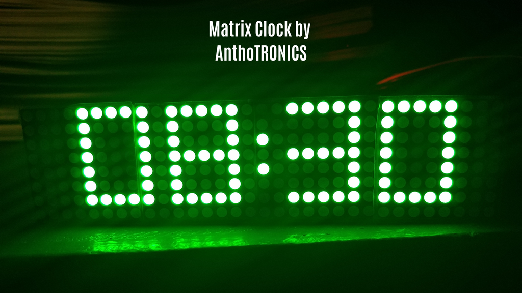
I want an NTP controlled clock for numerous projects.
Yes, I do need another clock in our Den and bedroom (with a projector), but I also need a thermostat for the mini-split AC in the shop and our irrigation controller.
So I got busy.
MAX7219 Vcc: 3.3 - 5V
|
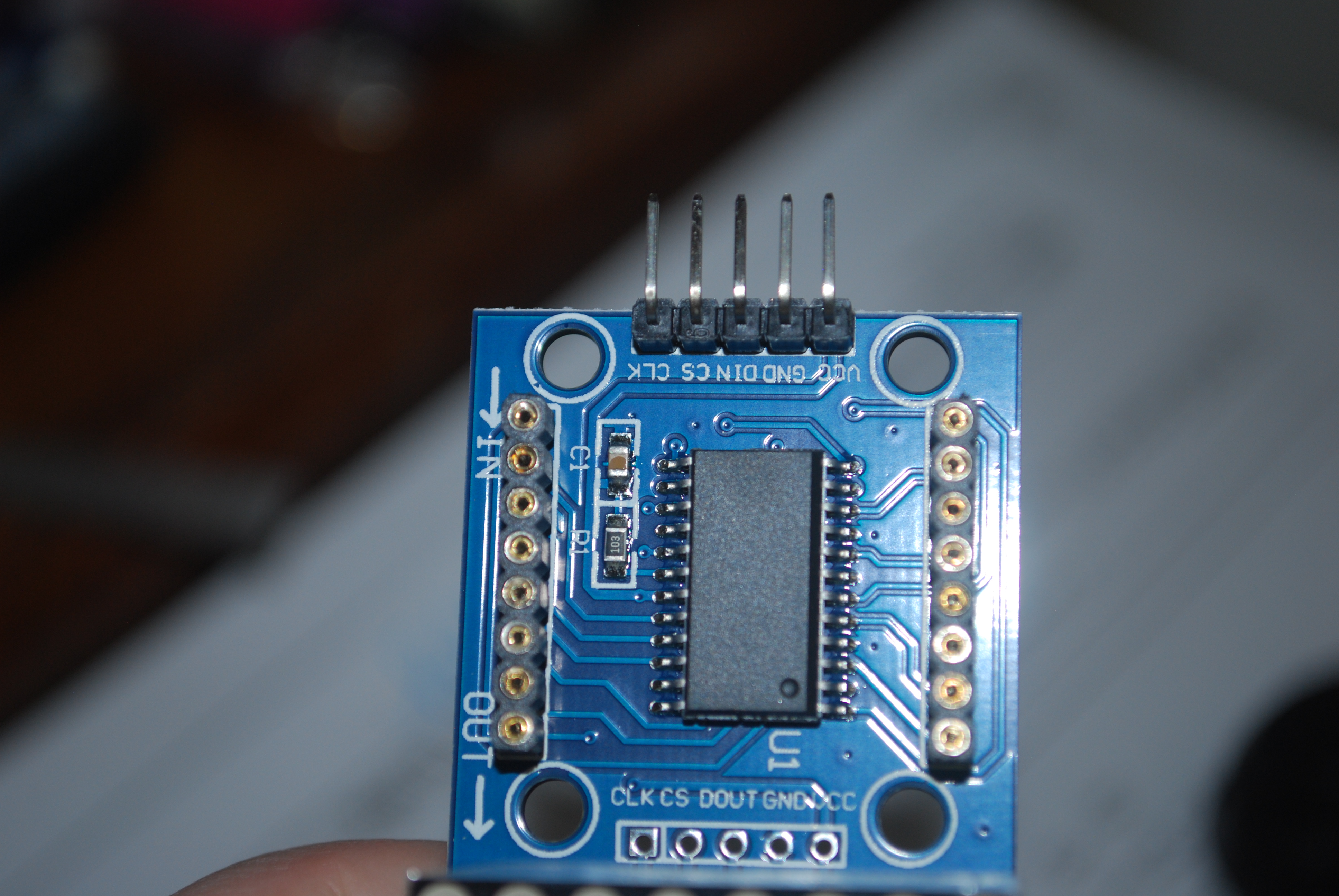
Bottom of a 32x8 LED MATRIX (MAX7219 control chip).
You can see the signal names (albeit upside down) on the main IO connector.
There are at least 3 types: Red: 1088AS ? Blu: 1088AB 46 Grn: 1088AYG |
| Sig | Nano | ESP32NodeMCU |
|---|---|---|
| Vin | 5V | 5V |
| Gnd | Gnd | Gnd |
| Din | D11 (MOSI) | 23 (vspi MOSI) |
| Clk | D13 (SCK) | 18 (vspi SCK) |
| Cs* | D7 | D7 |
| PARAMETER | SYMBOL | CONDITIONS | MIN TYP MAX | UNITS | |
|---|---|---|---|---|---|
| LOGIC INPUTS | |||||
| Input Current DIN, CLK, LOAD, CS | I IH , I IL | V IN = 0V or V+ | -1 1 | uA | |
| Logic High Input Voltage | V IH | 3.5 | V | ||
| Logic Low Input Voltage | V IL | 0.8 | V | ||
| Output High Voltage | V OH | DOUT, I SOURCE = -1mA | V+ - 1 | V | |
| Output Low Voltage | V OL | DOUT, I SINK = 1.6mA | 0.4 | V | |
| Hysteresis Voltage | ΔV I | DIN, CLK, LOAD, CS | 1 | V | |
| TIMING CHARACTERISTICS | |||||
| CLK Clock Period | t CP | 100 | ns | ||
| CLK Pulse Width High | t CH | 50 | ns | ||
| CLK Pulse Width Low t CL 50 ns CS Fall to SCLK Rise Setup Time (MAX7221 only) t CSS 25 ns CLK Rise to CS or LOAD Rise Hold Time t CSH 0 ns DIN Setup Time t DS 25 ns DIN Hold Time t DH 0 ns Output Data Propagation Delay t DO Load-Rising Edge to Next Clock Rising Edge (MAX7219 only) t LDCK 50 ns Minimum CS or LOAD Pulse High t CSW 50 ns Data-to-Segment Delay t DSPD www.maximintegrated.com C LOAD = 50pF 25 2.25 ns ms | |||||
|
|