The PN Junction As we know that p-type semiconductor has trivalent atoms and each of them produces one hole, we can visualize it as shown in the figure. Each circled minus sign is the trivalent atom and each plus sign is the hole in its valence orbit.
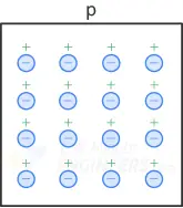 p type semiconductor
We also know that n-type semiconductor has pentavalent atoms and each of
them produces one free electron, we can visualize it as shown in the figure.
Each circled plus sign is the pentavalent atom and each minus sign is the
free electron it contributes.
p type semiconductor
We also know that n-type semiconductor has pentavalent atoms and each of
them produces one free electron, we can visualize it as shown in the figure.
Each circled plus sign is the pentavalent atom and each minus sign is the
free electron it contributes.
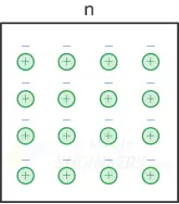 n type semiconductor
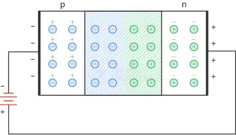
A manufacturer can produce a single silicon crystal with p-type material on
one side and n-type on the other side, as shown in the figure. The border
between p-type and n-type is called the PN junction.
n type semiconductor
A manufacturer can produce a single silicon crystal with p-type material on
one side and n-type on the other side, as shown in the figure. The border
between p-type and n-type is called the PN junction.
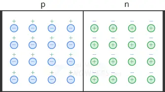 pn crystal
A PN crystal is commonly known as junction diode. The word diode is a
contraction of two electrodes, where di stands for two.
There are three possible biasing conditions for the PN Junction:
pn crystal
A PN crystal is commonly known as junction diode. The word diode is a
contraction of two electrodes, where di stands for two.
There are three possible biasing conditions for the PN Junction:
- Equilibrium or Zero Bias – No external voltage is applied to the PN junction.
- Reverse Bias – The positive source terminal is connected to the n-type, and the negative source terminal is connected to the p-type.
- Forward Bias – The negative source terminal is connected to the n-type, and the positive source terminal is connected to the p-type.
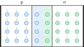
Equilibrium (zero bias) In a PN junction, without an external applied voltage, an equilibrium condition is reached. Let’s see how.
The Depletion Region An N-type semiconductor has a larger number of free electrons than a P-type semiconductor. Due to this high concentration of electrons on the N-side, they repel each other. Due to repulsion, free electrons spread (diffuse) in all directions. Some of them cross the junction. When a free electron enters the p region, it is attracted to the positive hole and recombines with it. When this happens, the hole disappears and the free electron becomes a valence electron. When the free electron falls into a hole on the P-side, the P-side atom gains an extra electron. The atom which gains an extra electron has more number of electrons than protons, due to which it becomes a negative ion. Ezoic Similarly, each free electron that leaves the N-side atom creates a hole in the N-side atom. The atom that loses an electron has more number of protons than electrons, due to which it becomes a positive ion. So each time an electron crosses the junction and recombines with a hole, it creates a pair of ions. Following figure shows these ions on each side of the junction.
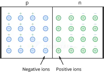 positive and negative ions at the junction
Each pair of positive and negative ions at the junction is called a dipole.
The creation of a dipole means that one free electron from the n-side and
one hole from the p-side are taken out of circulation. As the number of
dipoles builds up, the region near the junction is depleted of majority
charge carriers. Therefore we call this charge-empty region The depletion
region.
positive and negative ions at the junction
Each pair of positive and negative ions at the junction is called a dipole.
The creation of a dipole means that one free electron from the n-side and
one hole from the p-side are taken out of circulation. As the number of
dipoles builds up, the region near the junction is depleted of majority
charge carriers. Therefore we call this charge-empty region The depletion
region.
 depletion region
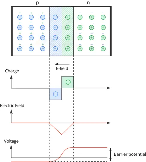
Barrier Potential Each dipole has an electric field between positive and negative ions. Whenever a free electron tries to enter the depletion region, this electric field pushes it back into the n region. The strength of the electric field increases with each electron-hole recombination inside the depletion region. Therefore the electric field eventually stops the diffusion of electrons across the junction and equilibrium is reached.
 barrier potential
The electric field between the ions is equivalent to a difference of
potential called the barrier potential. At room temperature, the barrier
potential equals approximately 0.3 V for germanium diodes and 0.7 V for
silicon diodes.
barrier potential
The electric field between the ions is equivalent to a difference of
potential called the barrier potential. At room temperature, the barrier
potential equals approximately 0.3 V for germanium diodes and 0.7 V for
silicon diodes.
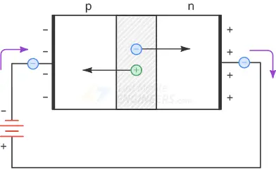
Forward Bias In forward bias, the p-type is connected with the positive source terminal and the n-type is connected with the negative source terminal. Following figure shows a forward bias diode.
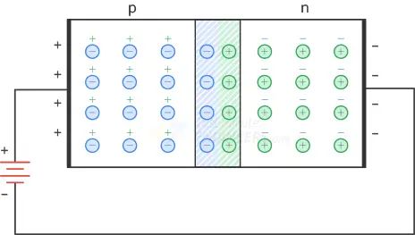 forward biased diode
With a battery connected this way, the holes in the p region and the free
electrons in the n region are pushed toward the junction. If the battery
voltage is less than the barrier potential (0.7V), the free electrons do not
have enough energy to get through the depletion layer. When they enter the
depletion layer, the ions will push them back into the n region. Because of
this, there is no current through the diode.
When the battery voltage is greater than the barrier potential (0.7V), the
free electrons have enough energy to pass through the depletion layer and
recombine with the holes. In this way they begin to neutralize the depletion
region, reducing its width.
Ezoic
When a free electron is recombined with a hole, it becomes a valence
electron. As a valence electron, it continues to travel to the left, passing
from one hole to the next until it reaches the left end of the diode. When
it leaves the left end of the diode, a new hole appears and the process
starts again. Since there are billions of electrons traveling at the same
time, we get a continuous current through the diode.
forward biased diode
With a battery connected this way, the holes in the p region and the free
electrons in the n region are pushed toward the junction. If the battery
voltage is less than the barrier potential (0.7V), the free electrons do not
have enough energy to get through the depletion layer. When they enter the
depletion layer, the ions will push them back into the n region. Because of
this, there is no current through the diode.
When the battery voltage is greater than the barrier potential (0.7V), the
free electrons have enough energy to pass through the depletion layer and
recombine with the holes. In this way they begin to neutralize the depletion
region, reducing its width.
Ezoic
When a free electron is recombined with a hole, it becomes a valence
electron. As a valence electron, it continues to travel to the left, passing
from one hole to the next until it reaches the left end of the diode. When
it leaves the left end of the diode, a new hole appears and the process
starts again. Since there are billions of electrons traveling at the same
time, we get a continuous current through the diode.
 flow of free electrons and holes
Reverse Bias Connecting the p-type to the negative terminal of the battery and the n-type to the positive terminal corresponds to reverse bias. Following figure shows a reverse bias diode.
 reverse biased diode
The negative battery terminal attracts holes, and the positive battery
terminal attracts free electrons. Because of this, holes and free electrons
flow away from the junction leaving the positive and negative ions behind.
Therefore, the depletion region gets wider.
Ezoic
The width of the depletion region is proportional to the reverse voltage. As
the reverse voltage increases, the depletion region gets wider. The
depletion region stops growing when its potential difference is equal to the
applied reverse voltage. When this happens, electrons and holes stop moving
away from the junction.
reverse biased diode
The negative battery terminal attracts holes, and the positive battery
terminal attracts free electrons. Because of this, holes and free electrons
flow away from the junction leaving the positive and negative ions behind.
Therefore, the depletion region gets wider.
Ezoic
The width of the depletion region is proportional to the reverse voltage. As
the reverse voltage increases, the depletion region gets wider. The
depletion region stops growing when its potential difference is equal to the
applied reverse voltage. When this happens, electrons and holes stop moving
away from the junction.
Reverse Current The reverse current in a diode consists of a minority-carrier current and a surface-leakage current. This reverse current is so small that you cannot even notice it and it is considered almost zero.
Reverse Saturation Current As we know that thermal energy continuously creates pairs of free electrons and holes. Suppose thermal energy has created a free electron and hole inside the depletion region. The depletion region pushes the newly created free electron into the n region, forcing it to leave the right end of the diode. When it reaches the right end of the diode, it enters the external wire and flows towards the positive battery terminal. On the other hand, the newly created hole is pushed into the p region. This extra hole on the p side allows one electron from the negative battery terminal to enter the left end of the diode and fall into a hole.
 reverse saturation current
Since thermal energy continuously produces electron-hole pairs inside the
depletion region, a small continuous current flows in the external circuit.
Such reverse current caused by the thermally produced minority carriers is
called the Saturation current. The name saturation means that increasing the
reverse voltage will not increase the number of thermally produced minority
carriers.
reverse saturation current
Since thermal energy continuously produces electron-hole pairs inside the
depletion region, a small continuous current flows in the external circuit.
Such reverse current caused by the thermally produced minority carriers is
called the Saturation current. The name saturation means that increasing the
reverse voltage will not increase the number of thermally produced minority
carriers.
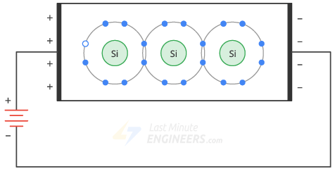
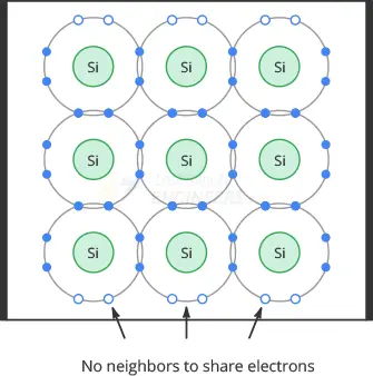
Surface-Leakage Current There exist another current in a reverse-biased diode. A small current flows on the surface of the crystal known as the Surface-leakage current. The atoms on the top and bottom surface of the crystal have no neighbors. They have only six electrons in the valence orbit. This means that each surface atom has two holes. The following image shows these holes along the surface of the crystal.
 surface leakage current
Due to this, electrons travel through the surface holes from the negative
battery terminal to the positive battery terminal. In this way, a small
reverse current flows along the surface.
surface leakage current
Due to this, electrons travel through the surface holes from the negative
battery terminal to the positive battery terminal. In this way, a small
reverse current flows along the surface.
Breakdown There is a limit to how much reverse voltage a diode can withstand before getting destroyed. If you continue to increase the reverse voltage, the diode will eventually reach the breakdown voltage. Once the breakdown voltage is reached, a large number of minority carriers are produced in the depletion region by Avalanche effect and the diode begins to conduct heavily in the reverse direction.
Avalanche Effect As we know there is a small minority-carrier current in a reverse-biased diode. When the reverse voltage increases, it forces minority carriers to move faster. These minority carriers moving at high speed collide with the atoms of the crystal and knock valence electrons loose, producing more free electrons. These new minority carriers join the existing minority carriers and collide with other atoms that knock off more electrons. One free electron dislodges one valence electron, resulting in two free electrons. These two free electrons then dislodge two more electrons, resulting in four free electrons. In this way the number of electrons increases in Geometric progression: 1, 2, 4, 8, . . .
 avalanche effect
This constant collision with atoms generates a large number of minority
carriers that produce a significant amount of reverse current in the diode.
And this process continues until the reverse current becomes large enough to
destroy the diode.
avalanche effect
This constant collision with atoms generates a large number of minority
carriers that produce a significant amount of reverse current in the diode.
And this process continues until the reverse current becomes large enough to
destroy the diode.
Diode Schematic Symbol Following figure shows the schematic symbol of a diode. The symbol looks like an arrow that points from the p side to the n side. The p side is called the anode and the n side the cathode.
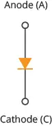 diode symbol
Diode I-V Characteristics Following figure shows a basic diode circuit in which the diode is forward biased. A series resistor RS is usually used to limit the amount of forward current IF.
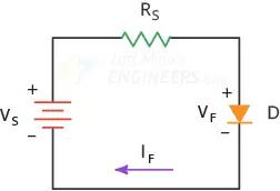 basic diode circuit
After connecting this circuit, if you measure the voltage and current of the
diode for forward and reverse bias, and plot it, you will get a graph that
looks like this:
basic diode circuit
After connecting this circuit, if you measure the voltage and current of the
diode for forward and reverse bias, and plot it, you will get a graph that
looks like this:
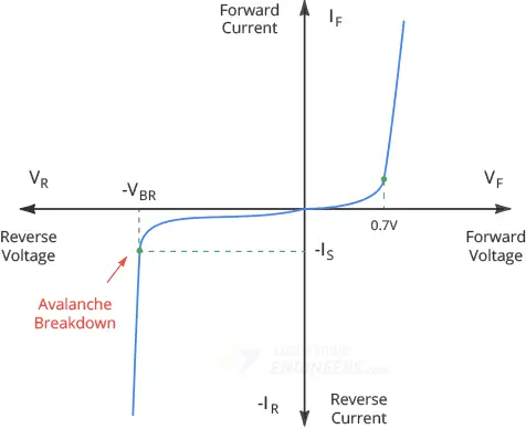 diode iv characteristics
This plot is called Current-Voltage (I-V) characteristics. This is the most
important diode characteristic because it defines how much current flows
through the diode for a given voltage.
A resistor is a linear device because its IV curve is a straight line. A
diode, however, is different. It is a nonlinear device as its IV curve is
not a straight line. This is due to the barrier potential.
Depending on the voltage applied across it, a diode will operate in one of
three regions: Forward bias, Reverse bias, and Breakdown.
diode iv characteristics
This plot is called Current-Voltage (I-V) characteristics. This is the most
important diode characteristic because it defines how much current flows
through the diode for a given voltage.
A resistor is a linear device because its IV curve is a straight line. A
diode, however, is different. It is a nonlinear device as its IV curve is
not a straight line. This is due to the barrier potential.
Depending on the voltage applied across it, a diode will operate in one of
three regions: Forward bias, Reverse bias, and Breakdown.
Forward Bias Region When the diode voltage is less than the barrier potential, a small current flows through the diode. When the diode voltage exceeds the barrier potential, the current flowing through the diode increases rapidly.
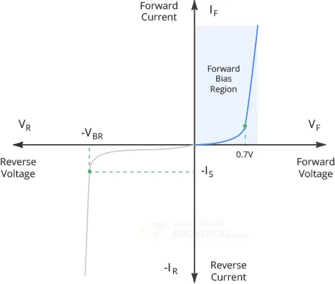 diode forward bias region
The voltage at which current starts to increase rapidly is called the
forward voltage (VF) of the diode. It is also called cut-in voltage or knee
voltage. Typically, a silicon diode has a VF around 0.7V and a germanium
-based diode has around 0.3V.
diode forward bias region
The voltage at which current starts to increase rapidly is called the
forward voltage (VF) of the diode. It is also called cut-in voltage or knee
voltage. Typically, a silicon diode has a VF around 0.7V and a germanium
-based diode has around 0.3V.
Reverse Bias Region The reverse bias region exists between zero current and breakdown. In this region, a small reverse current flows through the diode. This reverse current is caused by the thermally produced minority carriers. This reverse current is so small that you cannot even notice it and it is considered almost zero.
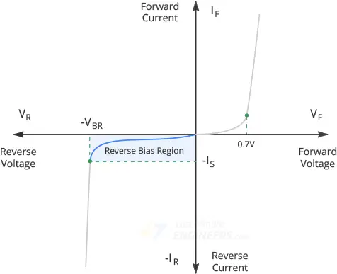 diode reverse bias region
Breakdown Region If you continue increasing the reverse voltage, you will eventually reach the so-called breakdown voltage of the diode. At this point, a process called Avalanche Breakdown occurs in the semiconductor depletion layer and the diode starts conducting heavily in the reverse direction, destroying the diode.
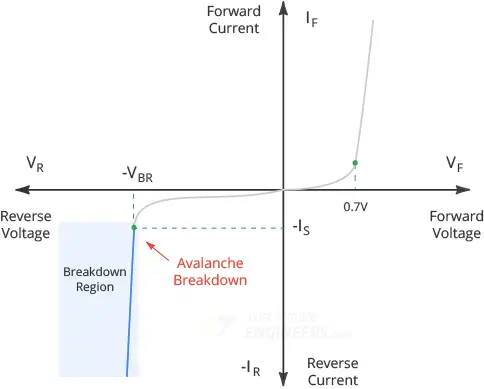 diode breakdown region
You can see from the graph that the breakdown has a very sharp knee,
followed by an almost vertical increase in current.
diode breakdown region
You can see from the graph that the breakdown has a very sharp knee,
followed by an almost vertical increase in current.