|
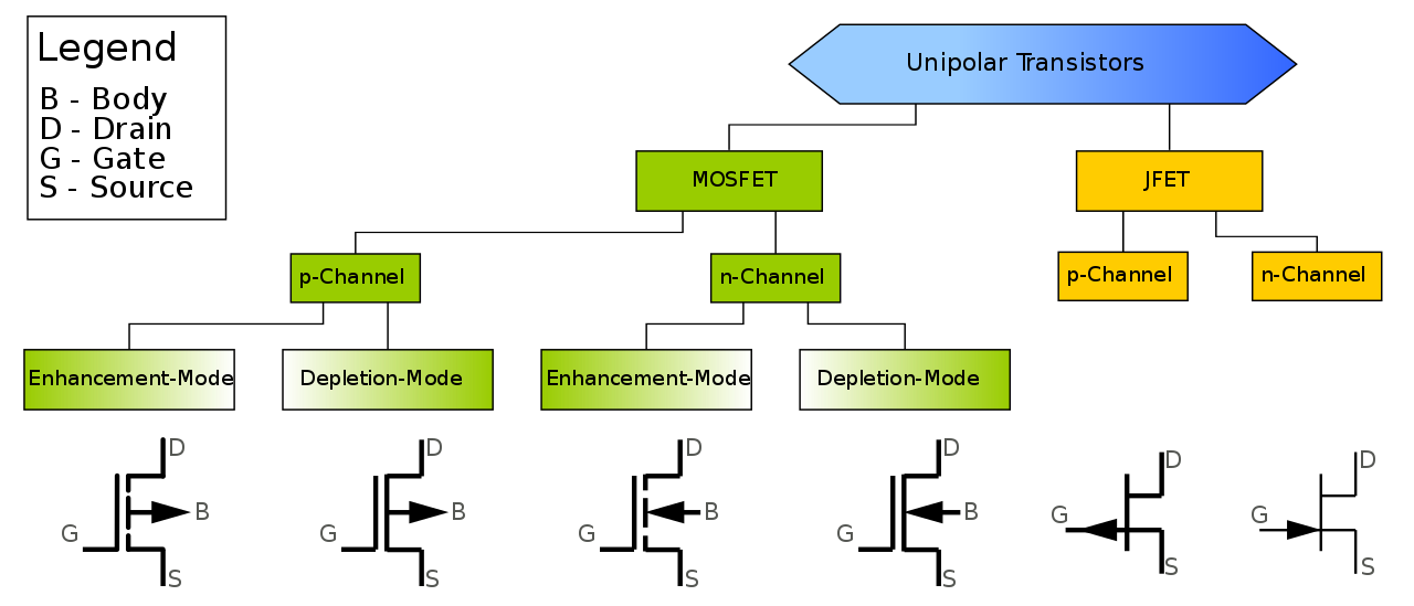
The channel of a FET is doped to produce either an n-type semiconductor or a
p-type semiconductor. The drain and source may be doped of opposite type to the
channel, in the case of enhancement mode FETs, or doped of similar type to the
channel as in depletion mode FETs. Field-effect transistors are also
distinguished by the method of insulation between channel and gate. Types of
FETs include:
- The MOSFET (metal–oxide–semiconductor field-effect transistor) utilizes an
insulator (typically SiO2) between the gate and the body. This is by far the
most common type of FET.
- The DGMOSFET (dual-gate MOSFET) or DGMOS, a MOSFET with two insulated gates.
- The IGBT (insulated-gate bipolar transistor) is a device for power control.
It has a structure akin to a MOSFET coupled with a bipolar-like main conduction
channel. These are commonly used for the 200–3000 V drain-to-source voltage
range of operation. Power MOSFETs are still the device of choice for
drain-to-source voltages of 1 to 200 V.
- The JLNT (Junctionless nanowire transistor) is a type of Field-effect
transistor (FET) which channel is one or multiple nanowires and does not present
any junction.
- The MNOS (metal–nitride–oxide–semiconductor transistor) utilizes a
nitride-oxide layer insulator between the gate and the body.
- The ISFET (ion-sensitive field-effect transistor) can be used to measure ion
concentrations in a solution; when the ion concentration (such as H+, see pH
electrode) changes, the current through the transistor will change accordingly.
- The BioFET (Biologically sensitive field-effect transistor) is a class of
sensors/biosensors based on ISFET technology which are utilized to detect
charged molecules; when a charged molecule is present, changes in the
electrostatic field at the BioFET surface result in a measurable change in
current through the transistor. These include enzyme modified FETs (EnFETs),
immunologically modified FETs (ImmunoFETs), gene-modified FETs (GenFETs),
DNAFETs, cell-based BioFETs (CPFETs), beetle/chip FETs (BeetleFETs), and FETs
based on ion-channels/protein binding.[46]
- The DNAFET (DNA field-effect transistor) is a specialized FET that acts as a
biosensor, by using a gate made of single-strand DNA molecules to detect
matching DNA strands.
- finFET, including GAAFET or gate-all-around FET, used on high density
processor chips
- The JFET (junction field-effect transistor) uses a reverse biased p–n
junction to separate the gate from the body.
- The static induction transistor (SIT) is a type of JFET with a short channel.
- The DEPFET is a FET formed in a fully depleted substrate and acts as a
sensor, amplifier and memory node at the same time. It can be used as an image
(photon) sensor.
- The FREDFET (fast-reverse or fast-recovery epitaxial diode FET) is a
specialized FET designed to provide a very fast recovery (turn-off) of the body
diode, making it convenient for driving inductive loads such as electric motors,
especially medium-powered brushless DC motors.
- The HIGFET (heterostructure insulated-gate field-effect transistor) is now
used mainly in research.[47]
- The MODFET (modulation-doped field-effect transistor) is a
high-electron-mobility transistor using a quantum well structure formed by
graded doping of the active region.
- The TFET (tunnel field-effect transistor) is based on band-to-band
tunneling.[48]
- The TQFET (topological quantum field-effect transistor) switches a 2D
material from dissipationless topological insulator ('on' state) to conventional
insulator ('off' state) using an applied electric field.[49]
- The HEMT (high-electron-mobility transistor), also called a HFET
(heterostructure FET), can be made using bandgap engineering in a ternary
semiconductor such as AlGaAs. The fully depleted wide-band-gap material forms
the isolation between gate and body.
- The MESFET (metal–semiconductor field-effect transistor) substitutes the p–n
junction of the JFET with a Schottky barrier; and is used in GaAs and other
III-V semiconductor materials.
- The NOMFET is a nanoparticle organic memory field-effect transistor.[50]
- The GNRFET (graphene nanoribbon field-effect transistor) uses a graphene
nanoribbon for its channel.[51]
- The VeSFET (vertical-slit field-effect transistor) is a square-shaped
junctionless FET with a narrow slit connecting the source and drain at opposite
corners. Two gates occupy the other corners, and control the current through
the slit.[52]
- The CNTFET (carbon nanotube field-effect transistor).
- The OFET (organic field-effect transistor) uses an organic semiconductor in
its channel.
- The QFET (quantum field effect transistor) takes advantage of quantum
tunneling to greatly increase the speed of transistor operation by eliminating
the traditional transistor's area of electron conduction.
- The SB-FET (Schottky-barrier field-effect transistor) is a field-effect
transistor with metallic source and drain contact electrodes, which create
Schottky barriers at both the source-channel and drain-channel interfaces.
[53][54]
- The GFET is a highly sensitive graphene-based field effect transistor used
as biosensors and chemical sensors. Due to the 2 dimensional structure of
graphene, along with its physical properties, GFETs offer increased sensitivity,
and reduced instances of 'false positives' in sensing applications[55]
- The Fe FET uses a ferroelectric between the gate, allowing the transistor to
retain its state in the absence of bias - such devices may have application as
non-volatile memory.
- VTFET, or Vertical-Transport Field-Effect Transistor, IBM's 2021
modification of finFET to allow higher density and lower power.[56]
|
|
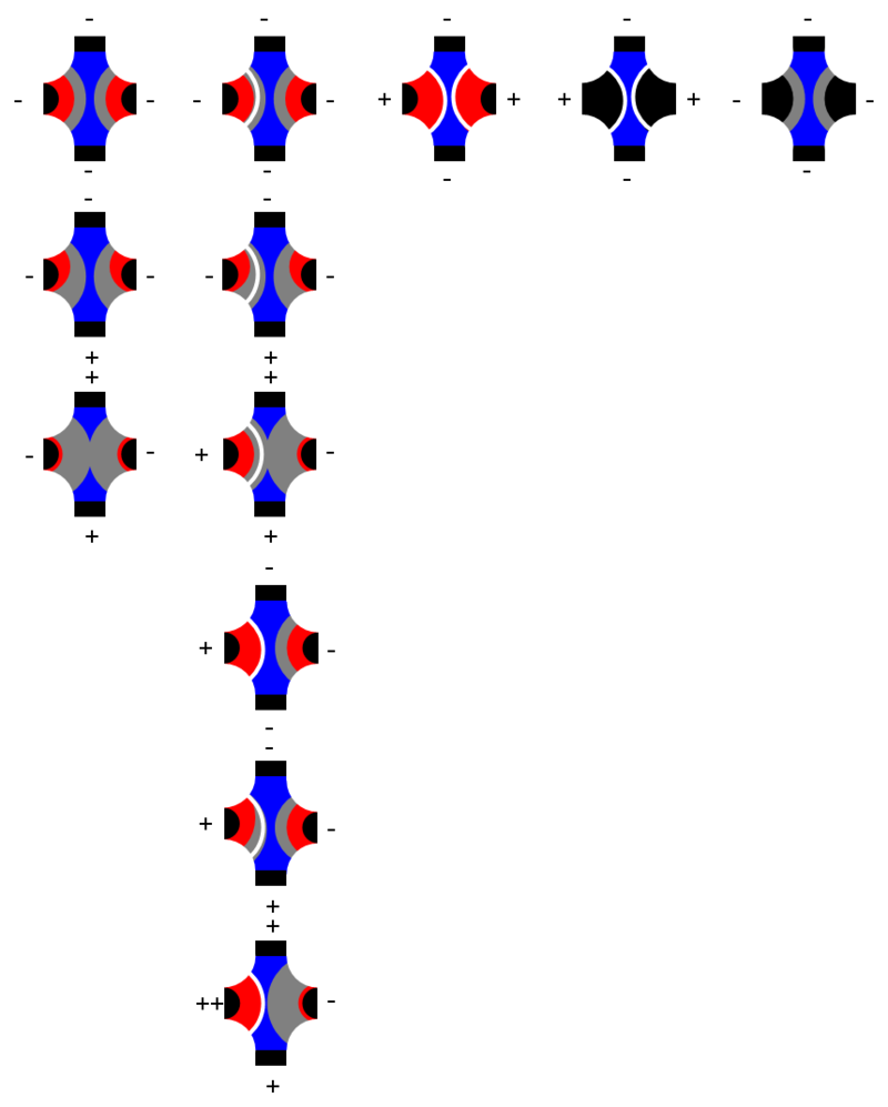
Depletion-type FETs under typical
voltages: JFET, poly-silicon MOSFET,
double-gate MOSFET, metal-gate MOSFET,
MESFET.
  Depletion
   Electrons
   Holes
   Metal
   Insulator
Top: source, bottom: drain, left: gate,
right: bulk. Voltages that lead to
channel formation are not shown.
|
|
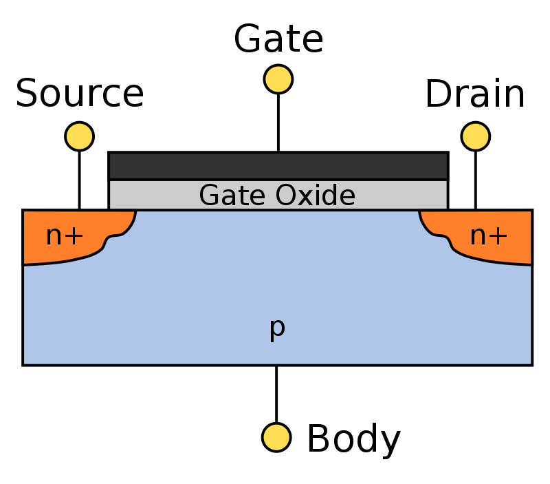
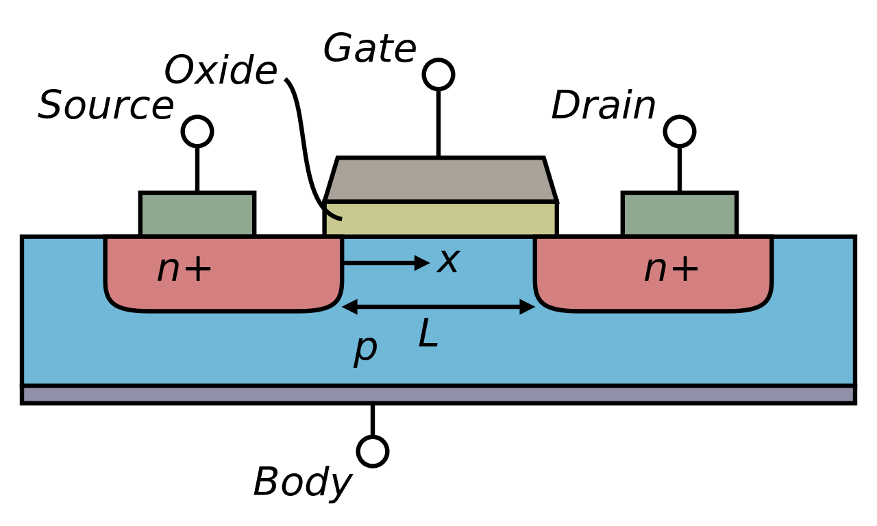 Cross section of an n-type MOSFET
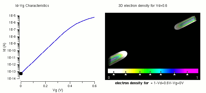
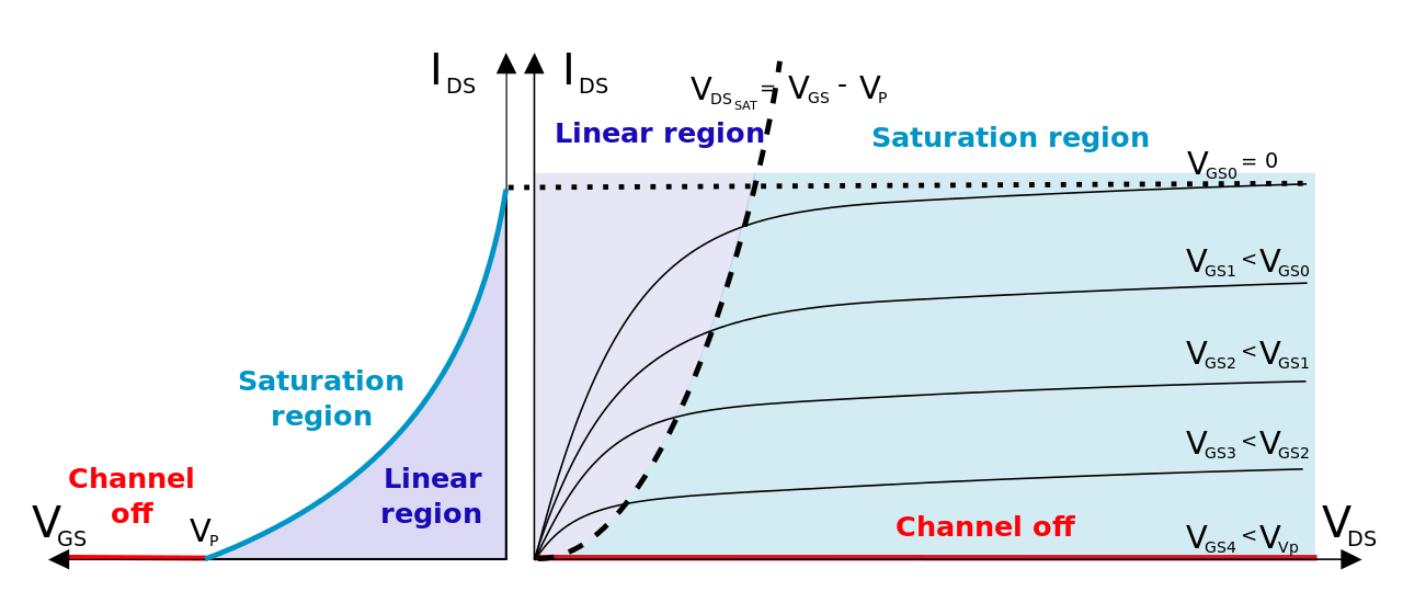 I–V characteristics and output plot of a JFET n-channel transistor