Conductor We all know that copper is a good conductor. The reason is obvious when we look at its atomic structure.
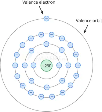 copper atom
The nucleus of a copper atom has 29 protons (positive charge). 29 electrons
(negative charge) revolve around the nucleus. There are 2 electrons in the
first orbit, 8 electrons in the second, 18 in the third and 1 electron in
the outer orbit.
In electronics, all that matters is the outer orbit , as it determines the
conductivity of the atom. It is also called valence orbit.
copper atom
The nucleus of a copper atom has 29 protons (positive charge). 29 electrons
(negative charge) revolve around the nucleus. There are 2 electrons in the
first orbit, 8 electrons in the second, 18 in the third and 1 electron in
the outer orbit.
In electronics, all that matters is the outer orbit , as it determines the
conductivity of the atom. It is also called valence orbit.
Net Charge To find the net charge of an atom, we define the core of an atom as the nucleus and all the inner orbitals. The core of a copper atom has a nucleus (+29 protons) and the first three orbits (-28 electrons). That’s why the core of a copper atom has a net charge of +1 (+29 of protons -28 of electrons) Following figure illustrates the core and the valence orbit of a copper atom.
 copper atom net charge
Free Electrons Because the core has a net charge of only +1, the attraction between the core and the valence electron is very weak. Even a nominal voltage can easily dislodge this electron from a copper atom and cause it to flow through the material. This is why the valence electron is often called a Free electron. And the flow of these free electrons is called Current. I think this diagram is a really good illustration of electron flow through a conductor. pt Number of free electrons in copper, as in other metals, is what makes it a good conductor of electricity.
Insulators Neon is an example of a best insulator. Let’s look at its atomic structure.
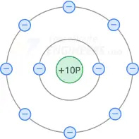 neon atom
A neon atom has 10 protons and 10 electrons. The first orbit contains two
electrons and the remaining eight electrons are in the valence orbit.
The core of a neon atom has a net charge of +8 because it contains 10 protons in
the nucleus and 2 electrons in the first orbit. Following figure shows the core
diagram of a neon atom.
neon atom
A neon atom has 10 protons and 10 electrons. The first orbit contains two
electrons and the remaining eight electrons are in the valence orbit.
The core of a neon atom has a net charge of +8 because it contains 10 protons in
the nucleus and 2 electrons in the first orbit. Following figure shows the core
diagram of a neon atom.
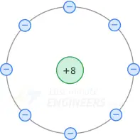 neon atom net charge
Because the core has a net charge of +8, the inward pull felt by the valence
electrons is very large. Therefore, due to lack of free electrons, insulators
do not conduct.
If a high enough voltage is applied to an insulator, the force is so great
that the valence electrons are literally torn from their atoms. This will cause
conduction. In the air you will see it as an arc or flash. In solid materials
the heat generated will char the material.
neon atom net charge
Because the core has a net charge of +8, the inward pull felt by the valence
electrons is very large. Therefore, due to lack of free electrons, insulators
do not conduct.
If a high enough voltage is applied to an insulator, the force is so great
that the valence electrons are literally torn from their atoms. This will cause
conduction. In the air you will see it as an arc or flash. In solid materials
the heat generated will char the material.
Semiconductor A semiconductor is an element that is neither a good conductor nor a good insulator. As you might expect, the best semiconductors have four valence electrons. Silicon is an example of a semiconductor. Let’s look at its atomic structure.
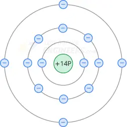 silicon atom
A silicon atom has 14 protons and 14 electrons. The first orbit contains two
electrons and the second orbit contains eight electrons. The four remaining
electrons are in the valence orbit.
The core of a silicon atom has a net charge of +4 because it contains 14
protons in the nucleus and 10 electrons in the first two orbits. Following
figure shows the core diagram of a silicon atom.
silicon atom
A silicon atom has 14 protons and 14 electrons. The first orbit contains two
electrons and the second orbit contains eight electrons. The four remaining
electrons are in the valence orbit.
The core of a silicon atom has a net charge of +4 because it contains 14
protons in the nucleus and 10 electrons in the first two orbits. Following
figure shows the core diagram of a silicon atom.
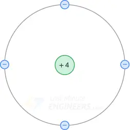 silicon atom net charge
The conductivity of the atom depends on the number of valence electrons.
When an atom has only one valence electron, it is a best conductor. When an
atom has eight valence electrons, the atom is a best insulator.
Ezoic
As you can see a silicon atom has four valence electrons due to which its
electrical conductivity falls between that of a conductor and an insulator.
This is what makes silicon a Semiconductor.
silicon atom net charge
The conductivity of the atom depends on the number of valence electrons.
When an atom has only one valence electron, it is a best conductor. When an
atom has eight valence electrons, the atom is a best insulator.
Ezoic
As you can see a silicon atom has four valence electrons due to which its
electrical conductivity falls between that of a conductor and an insulator.
This is what makes silicon a Semiconductor.
Silicon Crystals When silicon atoms combine to form a crystal, they arrange themselves in a systematic pattern. Each silicon atom shares its valence electrons with four neighboring atoms such that every atom has eight electrons in its valence orbit. The following figure shows how a silicon atom shares electrons with four neighbors.
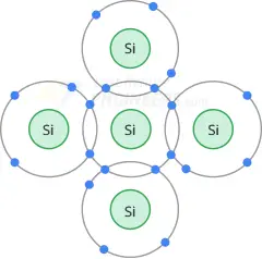 silicon crystal
Covalent Bonds Due to sharing, valence electrons no longer belong to any one atom. These shared valence electrons are pulled by neighboring atoms with equal and opposite forces, causing them to form a bond. We call this type of chemical bond a Covalent bond. The following figure shows the concept of covalent bonds where each straight line represents one shared electron.
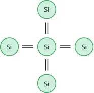 silicon covalent bonds
This pulling in opposite directions is what holds the silicon atoms together
and gives them solidity.
silicon covalent bonds
This pulling in opposite directions is what holds the silicon atoms together
and gives them solidity.
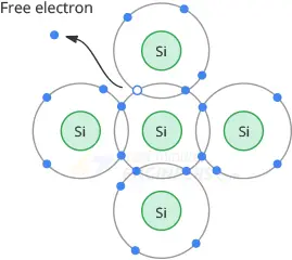
The Holes At room temperature, the thermal energy in the air causes the atoms in a silicon crystal to vibrate. These vibrations remove the electron from the valence orbit. This free electron starts moving randomly throughout the crystal. The departure of the electron creates a vacancy in the valence orbit called a hole. This hole behaves like a positive charge because the loss of an electron produces a positive ion.
 When a free electron enters the immediate vicinity of the hole, it is
attracted towards the hole and falls into it. The process of merging a free
electron and a hole is called Recombination.
When a free electron enters the immediate vicinity of the hole, it is
attracted towards the hole and falls into it. The process of merging a free
electron and a hole is called Recombination.
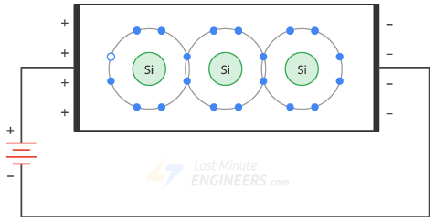
Flow of Free Electrons and Holes Let’s connect a battery across a pure silicon crystal. Assume that thermal energy has produced a free electron and a hole.
 flow of free electrons and holes
The applied voltage forces free electrons to flow to the left and holes to
the right. When free electrons reach the left end of the crystal, they enter
the external wire and flow towards the positive battery terminal.
On the other hand, free electrons at the negative battery terminal flow to
the right end of the crystal. They enter the crystal and recombine with
holes that have reached the right end of the crystal.
In this way, a steady flow of free electrons and holes is established inside
the semiconductor.
Free electrons and holes are often called Carriers because they carry a
charge from one place to another.
flow of free electrons and holes
The applied voltage forces free electrons to flow to the left and holes to
the right. When free electrons reach the left end of the crystal, they enter
the external wire and flow towards the positive battery terminal.
On the other hand, free electrons at the negative battery terminal flow to
the right end of the crystal. They enter the crystal and recombine with
holes that have reached the right end of the crystal.
In this way, a steady flow of free electrons and holes is established inside
the semiconductor.
Free electrons and holes are often called Carriers because they carry a
charge from one place to another.
Doping a Semiconductor In a pure silicon crystal, each silicon atom uses four valence electrons to bond with its neighboring atoms. This reduces the number of electrons available for conduction. Due to this it acts as an insulator. To increase the number of holes and free electrons in a silicon crystal, and thus to increase its conductivity, it is necessary to dope the crystal. Doping is the process of adding impurities to a pure silicon crystal to alter its electrical conductivity. And the impurity that is added is called a Dopant. The more impurities are added, the greater the number of free electrons and holes, resulting in an increase in conductivity. Meaning, a lightly closed semiconductor has a high resistance, while a heavily doped semiconductor has a low resistance. How is a silicon crystal doped? First a pure silicon crystal is melted. This breaks covalent bonds and transforms silicon from a solid to a liquid. To increase the number of free electrons, pentavalent atoms are added to the molten silicon. And to increase the number of holes, tritant atoms are added. Once it cools down, it turns into a solid crystal structure.
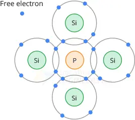
n-Type Semiconductor Silicon which is doped to increase the number of free electrons is called n-type semiconductor, where the n stands for negative. To increase the number of free electrons, pentavalent impurities such as phosphorus, antimony or arsenic are added to silicon. Pentavalent atoms, as the name suggests, have five valence electrons. Following figure shows a phosphorus atom.
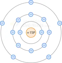 phosphorus atom
In n-type semiconductor, a pentavalent atom is in the center, surrounded by
four silicon atoms. As we know, a pentavalent atom has five valence
electrons. As before, neighboring silicon atoms share four electrons with a
pentavalent atom. But this time, there is an extra electron left over (Since
valence orbit can hold no more than eight electrons).
phosphorus atom
In n-type semiconductor, a pentavalent atom is in the center, surrounded by
four silicon atoms. As we know, a pentavalent atom has five valence
electrons. As before, neighboring silicon atoms share four electrons with a
pentavalent atom. But this time, there is an extra electron left over (Since
valence orbit can hold no more than eight electrons).
 n type semiconductor
Because each pentavalent atom in a silicon crystal produces one free
electron, the resulting doped material has a large number of free
electrons.
In an n-type semiconductor, as free electrons are greater in number than
holes, free electrons are called majority carriers and holes are called
minority carriers.
Ezoic
Because the pentavalent impurities donate an extra electron to the silicon
crystal, they are often referred to as donor impurities.
n type semiconductor
Because each pentavalent atom in a silicon crystal produces one free
electron, the resulting doped material has a large number of free
electrons.
In an n-type semiconductor, as free electrons are greater in number than
holes, free electrons are called majority carriers and holes are called
minority carriers.
Ezoic
Because the pentavalent impurities donate an extra electron to the silicon
crystal, they are often referred to as donor impurities.
p-Type Semiconductor Silicon which is doped to increase the number of holes is called p-type semiconductor, where the p stands for positive. To increase the number of holes, trialent impurities such as aluminum, boron, or gallium are added to silicon. Trivalent atoms, as the name suggests, have three valence electrons. Following figure shows a boron atom.
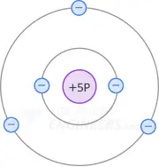 boron atom
In p-type semiconductor, a trivalent atom is in the center, surrounded by four
silicon atoms. Since the trivalent atom originally had only three valence
electrons and each neighbor shares one electron, only seven electrons are in the
valence orbit. This means that a hole exists in the valence orbit of each
trivalent atom.
boron atom
In p-type semiconductor, a trivalent atom is in the center, surrounded by four
silicon atoms. Since the trivalent atom originally had only three valence
electrons and each neighbor shares one electron, only seven electrons are in the
valence orbit. This means that a hole exists in the valence orbit of each
trivalent atom.
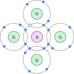 p type semiconductor
Because each trivalent atom in a silicon crystal produces one hole, the
resulting doped material has a large number of holes.
In an p-type semiconductor, as holes are greater in number than free
electrons, holes are called majority carriers and free electrons are called
minority carriers.
Ezoic
A trivalent atom is also called an acceptor atom, because each hole it
contributes, can accept a free electron during recombination.
p type semiconductor
Because each trivalent atom in a silicon crystal produces one hole, the
resulting doped material has a large number of holes.
In an p-type semiconductor, as holes are greater in number than free
electrons, holes are called majority carriers and free electrons are called
minority carriers.
Ezoic
A trivalent atom is also called an acceptor atom, because each hole it
contributes, can accept a free electron during recombination.
Going Further In the next tutorial, we will see how a single silicon crystal is doped with p-type material on one side and n-type on the other side to form a PN junction, which can be used to make a diode.